Key Highlights
-
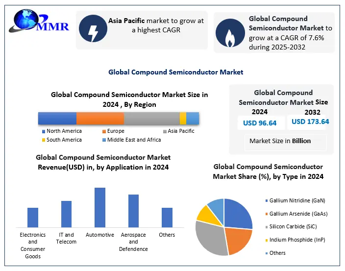
Market Capitalization Track: The industry valuation scales from USD 96.64 billion in 2024 to USD 173.64 billion by 2032, maintaining a steady 7.6% compound annual growth rate.
-
Material Composition Dominance: Silicon Carbide (SiC) stands as the dominant material type due to its extreme thermal conductivity and high-voltage efficiency within severe operational environments.
-
Product Architecture Leadership: The RF Power Devices segment leads product classifications, backed by a persistent global demand for high-frequency telecommunication hardware.
-
Application Sector Concentration: The IT and Telecom sector accounts for the largest application revenue share, driven by rapid continuous expansions of millimeter-wave 5G networks.
-
Geographic Production Engine: The Asia-Pacific region maintains the leading position in manufacturing capacity, backed by intensive electronics manufacturing services (EMS) infrastructure.
Why This Matters Now
Global foundry networks and electronics original equipment manufacturers (OEMs) face an immediate technological bottleneck as traditional silicon architectures hit fundamental physical limits in power density, thermal handling, and high-frequency transmission. Next-generation computing platforms, ultra-fast 5G networks, and high-voltage electric vehicle drivetrains demand rapid signal processing speeds and minimal energy loss that legacy silicon simply cannot provide.
Firms must alter their fabrication strategies toward advanced compound materials like Silicon Carbide and Gallium Nitride to capture premium industrial supply contracts. Foundries and fabless semiconductor operators that delay investments in wide-bandgap crystal growth and advanced packaging packaging lines risk losing structural competitiveness as global procurement policies shift permanently toward energy-efficient, high-frequency compound substrates.
Market Overview
The global Compound semiconductor market is transitioning from a specialized niche ecosystem into the standard foundation for high-power, high-frequency electronic engineering. Valued at USD 96.64 billion in 2024, the market is on a trajectory to reach USD 173.64 billion by 2032, achieving a 7.6% compound annual growth rate. This capital expansion marks a permanent shift in advanced component manufacturing, dictated by the superior electron mobility and wide bandgap properties of compound elements relative to standard silicon.
The core mechanics of this sector involve synthesizing two or more chemical elements from columns III and V, or II and VI of the periodic table, producing materials like Gallium Arsenide (GaAs), GaN, and SiC. These tailored chemical configurations allow devices to operate at significantly higher voltages, temperatures, and frequencies. As global industries implement rapid electrification frameworks and dense telecommunication networks, the demand for compound-based power modules and radio frequency (RF) components is disrupting legacy bills of materials (BOM) across the automotive, telecom, and aerospace industries.
Key Trends Driving Growth
The extensive commercial rollout of 5G telecommunications infrastructure and dense small-cell installations serves as a primary demand driver for the global market. Millimeter-wave 5G networks demand high-frequency operations and broad operational bandwidths to deliver ultra-fast data transmission speeds with minimal latency. Gallium Nitride and Gallium Arsenide compound semiconductors provide the high electron mobility required to build advanced RF power amplifiers, allowing base stations to maintain optimal transmission integrity while reducing total power consumption and heat dissipation.
Concurrently, structural supply chain developments are reshaping how industrial OEMs interact with wide-bandgap silicon foundries. The transition toward high-voltage electric vehicle architectures operating on 800-volt grids requires a massive supply of Silicon Carbide power inverters to minimize thermal losses and extend driving ranges. This automotive transition has triggered extensive multi-year procurement contracts and joint venture agreements between automotive OEMs and compound semiconductor fabs to guarantee stable wafer supplies amidst tight production capacities.
Segment Insights
-
Silicon Carbide (Dominant Material Segment): SiC commands the largest material revenue share of the global market. Exceptional thermal conductivity, massive high-voltage processing capacity, and superior energy efficiency make this material mandatory for electric vehicle power electronics, renewable energy grids, and heavy industrial power systems.
-
RF Power Devices (Dominant Product Segment): This product segment leads the marketplace due to the continuous installation of 5G hardware and advanced wireless communications infrastructure that demand reliable high-frequency performance.
-
IT and Telecom (Dominant Application Segment): This sector represents the primary application vertical for compound semiconductors. The explosive deployment of high-speed data centers, advanced optical communication networks, and localized cell arrays drives the continuous absorption of complex compound architectures.
Regional Growth Story
The Asia-Pacific region dominated the global compound semiconductor market in 2024, maintaining its position as the largest revenue and production contributor. This geographic concentration is supported by highly mature manufacturing ecosystems in Taiwan, South Korea, Japan, and China, alongside major cost-competitive advantages in high-volume chip packaging. However, rising labor costs in China and tightening international export controls are driving rapid regional rebalancing, prompting countries like Japan and India to provide substantial government incentives to build domestic semiconductor self-sufficiency.
In parallel, the United States is accelerating its domestic fabrication footprint through targeted corporate research funding and national security supply chain programs designed to shore up military and aerospace electronics production. European industrial hubs, led by manufacturing centers in Germany and Sweden, are focusing investment capital on specialized automotive power semiconductor fabs to support regional automotive assembly lines. These regional dynamics highlight a global shift toward manufacturing sovereignty, as major economies invest billions to decouple fragile component supply chains from geopolitical flashpoints.
Competitive Landscape
The global competitive ecosystem is characterized by heavy capital concentration, with established power electronics conglomerates and specialized substrate fabs fighting for dominance through aggressive capacity expansions. Prominent market entities include Cree Inc. (Wolfspeed), Freescale Semiconductor Inc., Mining & Chemical Products Ltd., Qorvo, Texas Instruments, Skyworks Solutions, International Quantum Epitaxy Plc., LM Ericsson Telefon AB, Infineon Technologies, and Broadcom Inc. Technology leadership belongs to organizations that can successfully transition from traditional 150mm (6-inch) wafer manufacturing to highly efficient 200mm (8-inch) SiC and GaN fabrication lines to drive down unit costs.
To secure long-term pricing power and defend their market shares, leading component suppliers are pursuing full vertical integration strategies, acquiring crystal growth facilities alongside fabless chip design operations. This trend toward structural integration allows top-tier players to optimize raw wafer yields, implement proprietary advanced packaging technologies, and provide comprehensive chiplet architectures to Tier-1 automotive and telecom customers. Furthermore, continuous capital investments in high-bandwidth memory (HBM) interfaces and edge-computing logic integration ensure that compound innovators maintain strong design-win momentum across the evolving AI data center market.
Recent Developments
-
Wide-bandgap fabrication leaders have finalized multi-million dollar plant modernizations to scale the commercial production of 200mm Silicon Carbide wafers, significantly increasing usable die counts per substrate.
-
Electronics manufacturing services providers have qualified next-generation Gallium Nitride power adapters that feature dual-stage power delivery in minimized physical form factors for consumer electronics.
-
Automotive engineering teams have successfully implemented integrated SiC power modules within production-line EV powertrain inverters, lowering thermal management requirements.
-
Government infrastructure agencies have approved major grants to co-fund open-access compound semiconductor research cleanrooms, aimed at accelerating commercialization cycles for fabless startups.
Strategic Implications
The permanent migration from elementary silicon to complex compound semiconductor fabrication introduces major manufacturing complexities and supply-chain variables for executive leadership. Synthesizing multi-element crystal structures requires exact process control and advanced epitaxy equipment, resulting in higher initial manufacturing defect rates and longer production cycles compared to legacy silicon ingots. Material providers and fab operators must invest heavily in automated defect detection systems and advanced metrology tools to improve factory yields and stabilize product margins.
Furthermore, the rising global focus on semiconductor sovereignty is forcing a complete reorganization of international component distribution channels. Corporate procurement managers can no longer rely on single-source offshore foundries for critical RF and power management chips without risking sudden regulatory bottlenecks or export restrictions. OEMs must cultivate multi-regional foundry relationships and localized advanced packaging alternatives, balancing manufacturing cost efficiencies against the strategic necessity of geopolitical supply-chain resilience.
Future Outlook
The global integration of compound semiconductor platforms will accelerate as industrial power grids, automated transport networks, and high-performance computing centers enforce strict energy-efficiency mandates. Future market progression will see wide-bandgap materials moving past isolated power modules into fully integrated, multi-material chiplet architectures where silicon logic gates sit directly alongside GaN RF components and SiC power nodes on a single packaging substrate. Ultimately, future market leadership will belong to vertically integrated chip manufacturers that control their own raw crystal growth pipelines and advanced packaging technologies, while laggards remain exposed to volatile wafer markets and shrinking margins on commoditized legacy silicon lines.
Analyst Perspective
“The compound semiconductor market has passed its initial validation phase and is now the core driver of high-voltage and high-frequency electronic engineering,” stated Rucha Deshpande, Lead Analyst at Maximize Market Research.
About Maximize Market Research
Maximize Market Research Pvt. Ltd. (MMR) is a global market research and consulting company that provides reliable, data-focused, and practical business insights. The firm serves a wide range of industries, including healthcare, pharmaceuticals, technology, automotive, electronics, chemicals, personal care, and consumer goods. Through market forecasts, competitive analysis, strategic consulting, and industry impact assessments, MMR helps organizations understand changing market conditions, identify growth opportunities, and make informed business decisions for long-term success.
2nd Floor, Navale IT Park Phase 3
Pune Banglore Highway, Narhe
Pune, Maharashtra 411041, India
+91 9607365656
[email protected]